Nanostructures on surfaces
Nanostructures on surfaces
Organic semiconducting films on metal/semiconductor surfaces
The last few decades organic semiconductors, and thin films of these, have attracted attention as they have been proven to be viable alternatives for conventional semiconductors in several electronical applications. Organic thin films have been used to create light emitting diodes, field effect transistors, solar cells, photodetectors, organic lasers, chemical- and biological sensors. These devices are all made of different layers of organic molecular films, conventional semiconductors and metals. The performance of these devices is highly dependent on the structure and quality of the organic films and the characteristics of the interface between the films and other materials in the devices. Therefore, a good understanding of the properties of thin films of organic semiconductors on various substrates is important for their use in electrical devices.
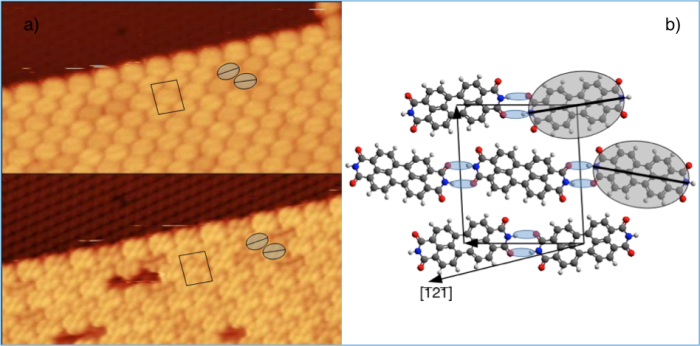
The organic semiconductor 3,4,9,10-perylene tetracarboxylic diimide (PTCDI) has recently attracted attention because it can be functionalized by exchanging hydrogens on the imide groups or the perylene core with other groups to tune its electrical, optical and charge-transport properties. The stronger interaction along the rows is N-H···O hydrogen bonding mediated by the imide groups. The weaker interactions between rows are hydrogen bonding between the oxygen, not involved in the stronger interaction, and hydrogen of the perylene core of a neighboring PTCDI. These two interactions are possible because the molecules in adjacent rows have slightly different orientations relative to the row direction. Here the growth of thin PTCDI films on the Ag/Si(111)-√3×√3 substrate has been studied with several PTCDI coverages. Each of these coverages was studied using scanning tunneling microscopy (STM).
a) STM images (size 10 nm x 20 nm), taken at two different biases (upper -2.0 V and lower 0.5 V), showing the edge of a 2D island. In both images the same unit cell is shown and two PTCDI molecules in neighboring rows are marked as “coffee beans” to illustrate their different orientations. b) Ball and stick model for the 2D structure of the PTCDI islands with the unit cell and its relation to the [121] substrate direction. The in-row hydrogen bondings are marked in blue and the oval with a central line added to two of the molecules corresponds to the "coffee beans" in a).

